 |
|
МЕНЮФестивали и конкурсы Семинары Издания О МОДНТ Приглашения Поздравляем НАУЧНЫЕ РАБОТЫ |
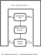
Реферат: Physical Methods of Speed-Independent Module DesignРеферат: Physical Methods of Speed-Independent Module DesignOleg Izosimov INTEC Ltd, Room 321, 7a Myagi Street, Samara 443093, Russia 1. Introduction Any method of logic circuit design is based on using formal models of gates and wires. The simplest model of a gate is determined by only two "parameters": (a) Boolean function is to be calculated, (b) fixed propagation delay. The simplest model of a wire is an ideal medium with zero resistance and consequently, with zero delay. Such simple models allow circuit design procedures which are a sequence of elementary steps easily realized by a computer. When logic circuits designed by using the simplest models expose unreliable operation as in the case of gate delay variations, designers introduce less convenient but more realistic models with arbitrary but finite delay. Using more complicated models may produce logic circuits that are called speed-independent [1]. In speed-independent circuits transition duration can be arbitrary. So a centralized clock cannot be used. Instead special circuitry to detect output validity is applied. Besides, additional interface circuitry is needed to communicate with the environment in a handshaking manner. A speed-independent circuit can be seen as a module consisting of combinational logic (CL) proper, CL output validity detector (OVD) and interface circuitry (Fig.1). To enable OVD to distinguish valid output data from invalid ones, the redundant coding scheme was proposed [2]. The main idea of the scheme is to enumerate all possible input and output data, both valid and invalid. The OVD must be provided with appropriate information on data validity. To realize the idea of redundant coding some constraints on CL design are imposed [3]:
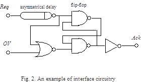
(i) CL must be free of delay hazards, i.e. CL output data word must not be dependent on the relative delay of signal paths through CL. (ii) In changing between input states, any intermediate or transient states that are passed through must not be mapped by CL onto valid output states. When these constraints were formulated, the circuit designers realised that not every Boolean description could be implemented in a speed-independent style. Other approaches to speed-independent module design were needed. SIM design as a science has two branches: logical and physical. For a long time physical branch was overshadowed in spite of its competitiveness. The main properties of physical approach to SIM design are: (a) Arbitrary coding scheme. (b) Conventional procedure of operational unit design. (c) Races of signals in SIM do not affect on its proper operation. In this paper we propose an approach based on the physical nature of transitions in CL. We believe that each transition is actually a transfer of energy which can be naturally detected by physical methods. From the viewpoint of a radio engineer CL behaves like a radio transmitter. It emits radio frequencies in the 108-1010Hz band modulated by signals of 106-108Hz. Obviously, the carrier wave is produced by gate switchings during transitions in CL. The modulating wave is produced by control schemes (OVD and interface circuitry) that detect transition completion and inform the environment about the readiness of CL. OVD is a kind of radio receiver that extracts the modulation envelope and enhances the received signal. The main properties that OVD circuit must expose from a radio engineer's point of view are selectivity and high gain. Since the useful signals can propagate through non-conducting medium, OVD circuits can be coupled with CL indirectly. Advances in semiconductor technology gave birth to two methods of transition detecting based on two kinds of the information carrying signal, namely electromagnetic radiation and current consumption. Frequency of the signal produced by switching logic gates is determined by gate delay. For instance, CMOS network of 1-ns gates produces 1-GHz signal, ECL array of 100-ps gates gives 10-GHz radiation. Logic circuits consisting of 10-ps gates will emit infra-red radiation. That signal could be easily detected by photosensitive devices. 2. Background Let us have a closer look at the structure of speed-independent modules (SIM) as presented in Fig.1. All input data are processed in CL, all output data are obtained from CL, too. So, CL is the only unit in SIM which is involved in proper data processing. The result of that processing is specified by Boolean functions. Algorithms for calculating the Boolean function are realised by the internal structure of CL. Generally, its structure is series-parallel as well as algorithm implemented. When n-bit data word is put into the CL, n or more signal propagation paths (SPPs) can be activated concurrently. So, one can say that the calculation of a Boolean function by CL is of parallel nature. On the other hand, each SPP is a gate chain which processes data in a serial manner. So, calculation in CL is also of sequential nature. The OVD circuit is intended for detecting transient and steady "states" of CL. If any SPP in CL is still "active", CL is in transient state, otherwise it is in steady state. Each gate switching results in both logical and electromagnetic effects on its surrounding medium. The logical effects of switching has been heavily investigated; we consider physical one. To provide speed-independence of the module the OVD and interface circuitry must also work in a speed-independent mode. This means that any arbitrary but finite transistor or wire delay cannot impair proper operation of OVD and interface circuitry. The interface circuitry is a mediator between OVD and environment of SIM. It implements any kind of signalling convention, commonly a two- or four-cycle one [4] based on request Req and acknowledgement Ack signal using. The interface circuitry receives the output validity (OV) signal from the OVD circuit, a Req signal from the environment and transmits an Ack signal to the environment (Fig.1). Consider an algorithm of operation for interface circuitry realizing speed-independent four-cycle signalling convention (FCSC). In accordance with FCSC the control signals must go in the following sequence: Req+OV-Ack+Req-Ack- where "+" corresponds to rising the signal and "-" corresponds to falling the signal. All signals are assumed to adhere to positive logic. Initially the signals Req and Ack are low, the signal OV is high. If the environment state changes, the Req signal rises and transient state of CL occurs (OV-). Upon completion of the transitions in CL, signal OV rises and the interface circuitry generates the Ack signal rising. After that the environment produces a falling Req signal and then the interface circuitry transmits the falling Ack signal to the environment. All the signals have to be reset into the initial state. To develop the interface circuitry a circuit designer must take into account that any OVD circuit has finite (non-zero) turn-on delay ton. This means that OVD cannot respond on transitions of short duration t tr< ton . An example of interface circuitry is shown in Fig.2. It contains a flip-flop, a NOR-gate, an asymmetrical delay and an inverter as an output stage [5].
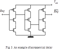
The asymmetrical delay is intended for delaying Req rising signal for + period where + > ton . Delaying Req falling signal noted - is to be as short as possible. Note that speed-independent operation of interface circuitry is vulnerable to delay + variation. If + becomes less than ton , proper operation of SIM can not be guaranteed. Otherwise, if + is much more than ton , performance of SIM will be significantly reduced. To provide exact accordance of + and ton a circuit emulator can be used. Such an emulator is either an exact copy of OVD or its functional copy, i.e. resistive-capacitive model of OVD's critical path. In the chip the emulator must be placed next to active OVD circuit in order to ensure identical conditions of fabrication and operation. In this example we use a simplified asymmetrical delay implemented as an asymmetrical CMOS inverter chain (Fig.3). Contrary to the common inverter an asymmetrical one has non-equal rise and fall times of output signal.
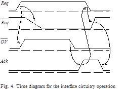
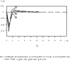
A time diagram for interface circuitry is presented in Fig.4 for two cases: (a) ttr < ton and (b) ttr ton. In case (a) the signal sequence Req+Ack+ is formed for (++tNOR) period where tNOR is a NOR-gate delay. In case (b) the above sequence is formed for (ttr +toff+tNOR) duration where toff is a turn-off delay of OVD circuit. When the SIM returns to the initial steady state, the signal sequence Req-Ack- is formed for (-+tNOR) interval.
After considering the SIM in operation it is obvious that the main problems of the module design are in the area of CL and OVD interaction. This includes (a) kind of signal used as a carrier of information about CL output validity, and (b) method of OVD circuit design. 4. Current consumption detection Using current consumption of CMOS CL for output validity detection was proposed in 1990 [7]. Contrary to the method of EMR detection this one is based on introducing direct coupling of source and receiver. While CL is in steady state it consumes current of about 10-9-10-8A which does not allow OVD switching. The interface circuitry gets information on CL output validity and in turn informs the environment about CL readiness to input data processing. When an input data arrives CL changes its state to "transient", current consumption increases to 10-4-10-2A, which switches the OVD, thus informing the interface circuitry about output invalidity. The latter lets the environment know about CL business. After the computations in the CL are finished, the current consumption decreases down to the steady state value, and the OVD sends a signal of output validity. 4.1 Information carrying signal Current consumption by CMOS CL contains useful information on CL state. CMOS CL is a network of CMOS gates, so the current consumed by CL is a superposition of currents consumed by CMOS gates included in the CL. Each CMOS gate contains PMOS transistor and NMOS transistor networks (Fig.5). While a gate is in a steady state either the PMOS or the NMOS network is in a conducting mode. When a gate switches the non-conducting transistor network becomes conducting. There is usually a short period in switching time when both networks are in a conducting mode.
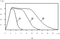
Generally, current consumed by a CMOS gate includes three components [9,10]: (a) leakage current Ilk passing between power supply and ground due to finite resistance of non-conducting transistor network; (b) short-circuit current Isc flowing while both networks are in a conducting mode; (c) load capacitance CL charge current ILC flowing while a CMOS gate is switching from low to high output voltage via conducting PMOS network and CL . SPICE simulation has shown [5] that amplitude of current consumed by a typical CMOS inverter depends on CL and is limited by the non-zero resistance of the conducting PMOS network (Fig.7). The integral of consumed current is proportional to CL . When a gate switches from high to low output voltage, the component ILC is negative by direction and negligible by value (Fig.7b). It is evident, the switchings from high to low output voltage occur at the expense of energy accumulated in CL during the previous switching from low to high output voltage. The component Isc does not depend on direction in which a gate switches.
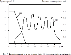
The component ILC equals to ILC = CLVdd f where Vdd is a power supply voltage, f is a gate switching frequency. Veendrick has investigated the component Isc dependencies on CL and rise-fall time of input potential signal [10]. He showed that if both input and output signal have the same rise-fall time, the component Isc cannot be more than 20 percent of summary current consumption [10]. However, when the output signal rise-fall time is less than input one, the component Isc can be of the same order of magnitude as ILC. In that case it must be taken into account. As to the component Ilk, it entirely depends on CMOS process parameters and for state of the art CMOS devices Ilk is about 10-15 -10-12 A. So, the analysis of CMOS gate current consumption allows us to conclude that in transient state a CMOS gate consumes a current I= Ilk+Isc+ILC and in steady state it consumes only Ilk<< I . The difference between two states from the viewpoint of current consumption is several orders of magnitude. So, CMOS gate output validity detection is possible, both in principle and in practice. In Section 2 we presented series-parallel model of computations in CL. We showed that in every moment during switching current consumed by CL is a superposition of the currents consumed on the activated signal propagation paths (SPPs). Now, considering CL implemented by CMOS devices we should note that while logical signal propagates through SPP the neighbouring gates switch in opposite directions. That is why a curve of current consumed by a ten inverter chain (Fig.8) looks like a combination of crests and troughs. Nevertheless, in the very lowest point of the curve the current consumed by CL in a transient state remains several orders more than in a steady state.
4.2 OVD implementation The proposed OVD circuit, shown in Fig.9, is a threshold circuit translating an analog current signal I into a logical signal OV.
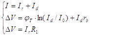
The OVD circuit contains a current-to-voltage converter (CVC) consisting of the resistor R1 and the diode D1. The OVD also contains a comparator implemented by the MOS transistors M1-M7 and resistors R2,,,R3 . CMOS CL consumes the current I and introduces a capacitance Cin . The capacitance Cout represents the load caused by the interface circuitry. A low potential output signal of OVD corresponds to CL output validity. A high potential output signal corresponds to CL output invalidity. So, OVD generates OV signal in negative logic manner. The transfer characteristics of CVC is determined by a system of three equations:
where I is an input
current of CVC, V is a voltage drop on the
CVC circuit, Ir is
a current flowing through the resistor R1, Id is a
current passing through the diode D1, I0 is a
leakage current of the diode, rb is a bulk resistance of the
diode. Here Equations
(1)-(3) determine the functional connection F between input current I
and voltage drop V:
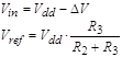
CVC parameters to be calculated are R1 and rb. Initial data for calculating R1 are the threshold voltage drop Vth and corresponding threshold input current Ith . Value Ith is determined by minimal current consumed by CMOS CL in transient state. Initial data for calculating rb are maximal voltage drop Vmax and corresponding maximal input current Imax. Value Imax is determined by the maximal number of gates in CL switching simultaneously and their load capacitances. The comparator chosen is the CMOS ECL receiver proposed by Chappell et al.[11]. The circuit includes a single differential amplifier stage with built-in compensation for parameter variations, followed by a CMOS inverter. The comparator has 100-mV worst-case sensitivity in 1-m technology. Detailed static and dynamic analysis of the comparator circuit was given in [11]. The comparator compares input voltage signal Vin with reference voltage Vref. If Vin <Vref the comparator output signal equals to logical zero which means that CL outputs are valid. Otherwise, Vin >Vref, the comparator output signal equals to logical "one" which means that the outputs are invalid. As it follows from the OVD circuit configuration, where Vdd is a voltage of power supply. Equations (4) and (5) allow us to calculate the threshold voltage drop V of the CVC circuit: since
If 0<V<500mV then the diode D1 of CVC operates in the very small current region Id 0 and Id <<Ir. So the component Id in the Equation (1) can be neglected and IIr =V/R1 . For practical
values of Страницы: 1, 2 |
Приглашения09.12.2013 - 16.12.2013 Международный конкурс хореографического искусства в рамках Международного фестиваля искусств «РОЖДЕСТВЕНСКАЯ АНДОРРА»09.12.2013 - 16.12.2013 Международный конкурс хорового искусства в АНДОРРЕ «РОЖДЕСТВЕНСКАЯ АНДОРРА»
|


Copyright © 2012 г.
При использовании материалов - ссылка на сайт обязательна.